
MODELING STUDY OF
LASER BEAM SCATTERING BY DEFECTS ON SEMICONDUCTOR WAFERS
Srikumar Sandeep1 and
Alexander Kokhanovsky2
1Ecole Polytechnique,
Montreal, Canada 2University of Bremen, Germany
ABSTRACT
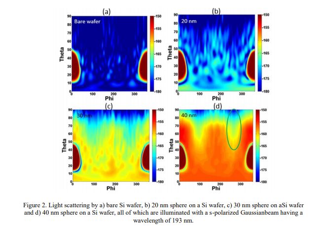
Accurate modeling of light
scattering from nanometer scale defects on Silicon wafersiscritical for
enabling increasingly shrinking semiconductor technology nodes of the future.
Yet, such modeling of defect scattering remains unsolved since existing
modeling techniques fail to account for complex defect and wafer geometries.
Here, we present results of laser beam scattering from spherical and
ellipsoidal particles located on the surface of a silicon wafer. A commercially
available electromagnetic field solver (HFSS) was deployed on a multiprocessor
cluster to obtain results with previously unknown accuracy down to light
scattering intensity of -170 dB. We compute three dimensional scattering
patterns of silicon nanospheres located on a semiconductor wafer for both
perpendicular and parallel polarization and show the effect of sphere size on
scattering. We further computer scattering patterns of nanometer scale
ellipsoidal particles having different orientation angles and unveil the
effects of ellipsoidal orientation on scattering.
KEYWORDS
Defect, Laser, Scattering,
Semiconductor, Wafer, Gaussian beam, HFS


Comments
Post a Comment